
 E-mail
 Print
Print facebook
 twitter
 Linkedin
 google+
1 Introduction
The development speed and demand for microchips continue to increase. Semiconductor manufacturers need stable production yields, but the ability to produce microchips in large quantities is the biggest issue [1ŌĆō3]. The machines in each process of semiconductor manufacturing are very complex and difficult to maintain and calibrate to achieve a high yield of production output [4]. The zero-defect manufacturing (ZDM) approach was proposed to decrease the failures in the semiconductor manufacturing processes. ZDM investigates three methods: detection, repair and prediction, and prevention [2]. Furthermore, ZDM can be implemented in product and process-oriented directions. The product-oriented approach detects defects that have occurred and belongs to a part of the detection class. This approach already applies to five types of semiconductor manufacturing machines [5]: plasma-etching, chemical vapor deposition (CVD), plasma-enhanced chemical vapor deposition (PECVD), chemical-mechanical planarization (CMP), and photolithography. The product-oriented approach mainly focuses on product quality directly from process data to estimate the characteristics and exploits data-driven algorithms to detect defects. However, process quality is still a major task in achieving optimal yields and controlling the process variability to satisfy the performance of multiple chambers.
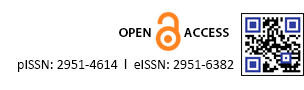
This paper presented an innovative framework for predictive metrology with a 5-level Cyber-Physical System (CPS) architecture to address the process quality issue. The architecture can collect process data from the golden machine (high yield machine specified by process engineers and original equipment manufacturers [6]) and extract features to train the golden machine model. After golden machine modeling, all target machines can compare with the golden machine using a pear-to-pear transfer learning algorithm. Take the plasma-etching machine as an example; the value of the etching rate can be predicted to compare chamber-to-chamber discrepancy. The whole process can be called predictive metrology (PM). The contribution and novelties of this paper can be shown as the following:
The predictive metrology (PM) concept is presented to address the task of process quality, reduce process variability, and virtually predict the output values, such as material removal rate, etching rate, etc., using pear-to-pear transfer learning.
5-level CPS structure is utilized to implement this concept in the semiconductor manufacturing field, ensuring product yield and quality. 5C architecture can inspect each level to find out which level has a problem and repair it immediately.
The rest of this paper is organized as follows: Section 2 introduces the 5C Cyber-Physical System (CPS) architecture in semiconductor manufacturing. Section 3 presents the proposed predictive metrology (PM) framework implementation. Section 4 demonstrates the case study using the proposed framework. The conclusions are given in Section 5.
2 5C Architecture in the Semiconductor Manufacturing Process
The 5-level Cyber-Physical System (CPS) structure has been widely implemented in different industrial scenarios [7,8]. Considering the application of semiconductor manufacturing which requires a close connection of the 5C architecture to convert big data into useful information to help the production and manufacturing upgrade of the semiconductor industry. Fig. 1 shows the flowchart of predictive metrology with 5-level CPS architecture. The 5C architecture applied at each level of semiconductor manufacturing provides a detailed explanation as follows.
2.1 Smart Connection Level
In order to obtain the measurement data during the process in the semiconductor machine, it is necessary to install highly reliable different types of sensors to collect a large amount of data. The collected measurement data can be stored in the local data center. The data collected by different kinds of machines in other regions or countries through networks and the cloud can be stored in the central data monitoring server. Thus, there are two key considerations in the first level, one is to select suitable sensors, and the other is to store different kinds of data in the centers and servers.
2.2 Data-to-Information Conversion Level
Correlation between the metrology parameters, process parameters and sensor data are established at this level. The data collected by the golden machine can be converted into valuable information at this level based on feature engineering. The golden machine can be modeled using machine learning algorithms based on extracted features. More detail about the steps involved at this level is discussed in the Section 3.
2.3 Cyber Level
The data information from all target machines can be collected together in central monitoring server at the cyber level. Utilizing the potential of transfer learning, golden machine modeling can be compared with all target machines, and predictive metrology parameters such as material removal rate, etching rate, etc., can be predicted. This step performs the peer-to-peer comparison and also called chamber-to-chamber discrepancy detection, where the predicted value from the golden machine can be compared and rated among the target machines. The cyber level presents all target machines with self-comparison ability.
2.4 Cognition Level
After the cyber level generates the virtual prediction of metrology parameters, the cognition level generates the total feedback matching error acquired by comparing the server database and virtual prediction value. The cognition level collects the total feedback matching error and shows the visualization function, including the comparative information between target machines and the server database. Visualization demonstrates useful quantitative information to give appropriate approaches to performing machine calibration.
2.5 Configuration Level
The function of the configuration level is to acquire feedback from cyberspace to the physical space. Total feedback matching errors from the cognition level can be regarded as a reference to assist administrators who can recalibrate the machine to maintain the total product yield and product quality. The configuration level also performs the alert function when the virtual metrology result is different from the expectation.
3 Systematic Implementation of Predictive Metrology in CPS Architecture
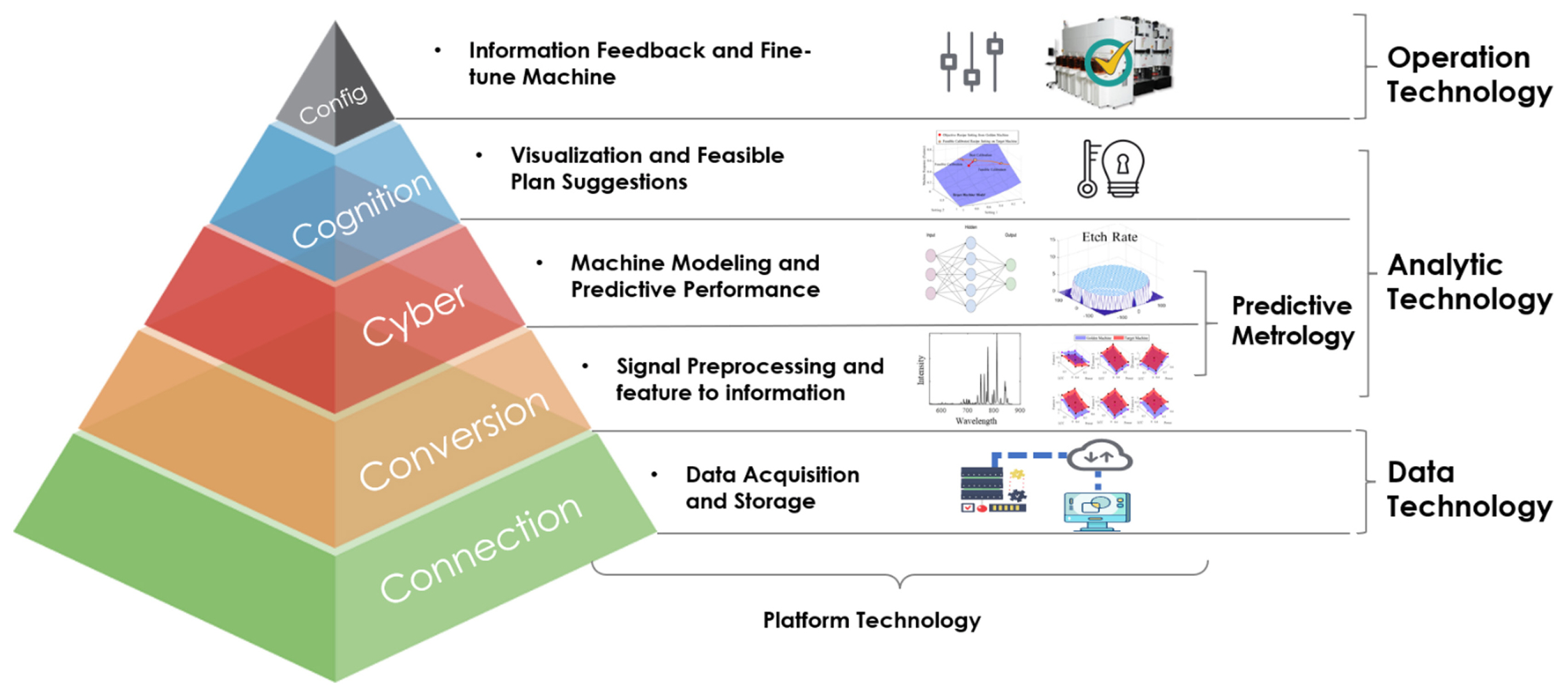
The core part of predictive metrology focuses on the conversion level and cyber level inside CPS architecture. Fig. 2 shows details about the technology adopted inside these two levels.
3.1 Signal Preprocessing
Signal preprocessing is a technique that can extract information from the original raw sensor dataset. It is also required before the feature engineering [9,10]. Because of the fluctuation of sensors and measuring environment, there might be some missing data and outlier data. The main purpose of the signal preprocessing step is to remove the outliers and compensate for the missing data to enhance the accuracy of modeling. The outlier is generally understood as the observations deviating from the majority. Outlier detection can be divided into three categories: supervised, semi-supervised, and unsupervised. In the semiconductor area, unsupervised detection is the most common method.
Missing data is a common occurrence when collecting the signal and can impact the modeling results. There are mainly three ways to solve the missing data issue, the first one is imputation, which means filling the missing values; the second is omission, which means discarding the samples containing the missing value; the third is analysis, which means applying the models which are not affected by missing values. In the semiconductor area, it is normal to use the second method, discarding the samples containing the missing values.
3.2 Feature Engineering
Feature engineering is a technique that extracts useful information based on domain knowledge from the original dataset and selects the ones with a high positive contribution to the models [11]. A suitable method in feature engineering is directly related to the modelŌĆÖs accuracy. In a basic view, feature engineering can be divided into three parts, feature extraction, feature selection, and feature fusion.
Feature extraction is to extract the information from the original dataset. The main focus of feature extraction is to find a suitable representation of multivariate data [12]. For different types of machines, the feature extraction method is different. But basically, extracting the statistical feature is one of the universal methods. After extracting features from the original data, it is common that these features are in high dimension. Some features are irrelevant or misleading, which can be detrimental to the model prediction [13]. Therefore, selecting specific features from the original feature space is vital to the modelŌĆÖs accuracy.
There are many methods for selecting the best features based on calculating the relationship between features and labels, such as Pearson correlation coefficient, intraclass correlation, and spearmanŌĆÖs rank correlation coefficient [14]. It is hard to tell which methods suit the semiconductor area directly. Therefore, it is necessary to do experiments based on these methods. There are usually more than two domains in the semiconductor area, which are commonly known as the source domain and the target domain [15]. Because the machine settings are different between the source and target domains, it is necessary to find the cross-domain features. Cross-domain feature selection is a core part of predictive metrology.
After selecting the best features, the feature matrix may still be in a high dimension. Sometimes, building an accurate model based on these high dimensional best features is hard. Therefore, feature fusion is extremely important during the modeling process. Principal Component Analysis (PCA) is one of the most widely used method in the semiconductor area. PCA method can decrease the redundancy and maximize the information obtained from the original information [16].
3.3 Machine Modeling
The golden machine is defined as high-yield referenced machines specified by process engineers and original equipment manufacturers (OEMs) [6]. Whereas, the target machine usually experienced issues such as sensor drift, component degradation, etc. In golden machine labeled data sample is larger than the target machine. Therefore, it is easier to obtain an accurate golden machine model than the target machine modeling. There are usually discrepancies between the golden machine and the target machine. These discrepancies affect the product quality and produce low yield. Chamber matching is a common practice to harness these discrepancies and calibrate the machine accordingly. Since poor machine modeling affects the effectiveness of chamber matching, building an accurate golden machine model and target machine model, which can show the discrepancies between two machines, is important when doing chamber matching.
Machine modeling means building a model representing the relationship between features and labels. During modeling, it is necessary to get enough high-quality data to ensure the robustness of the model. However, in the semiconductor area, because of the high cost of obtaining/measuring data, the target domain lacks labeled data or no labeled data [17]. Building the model directly based on target machine data will have low accuracy. Therefore, using multi-task learning or domain adaptation technology for the target machine based on golden machine modelling is necessary.
Golden machine modeling is based on the golden machine domain features and labels. The golden machine is the one that has high yield performance designed by process engineers and original equipment manufacturers [6]. The golden machine usually contains enough labeled data. Therefore, the golden machine model can be a data-driven or physical-based model.
A lot of research is focused on how to improve the accuracy of the target machine model. Transfer learning is a common adaptation method. The basic idea is to transfer model parameters obtained from the golden machine to the target machine. Simply transferring model parameters will achieve a low accuracy. Therefore, Kang et al. [18] proposed a feature-selection-based transfer learning method, Moslem et al. [19] proposed a deep learning-based domain adaptation technology to improve accuracy.
3.4 Predictive Performance
The main goal of PM is to control product quality based on process data. The metrology parameterŌĆÖ prediction value plays the interconnect between the process data and product quality. In other words, this prediction value is determined by the process and shows the product quality. For example, in the Chemical-mechanical planarization (CMP) application, the material removal rate (MRR) prediction value is the metrology parameter. Similarly, in the plasma-etching machine, it is the etching rate. Based on these predictions, model performance needs to be evaluated. Different models have different criteria to evaluate, but the mean square error (MSE) and regression value are the most common methods to test the performance. Setting suitable criteria is vital to the model evaluation.
3.5 Peer-to-Peer Comparison
The comparison between the golden and target models is called peer-to-peer comparison. Peer-to-peer comparison in the cyber-physical system was developed in 2015 [7]. In the semiconductor area, peer-to-peer comparison means that when target machines arrive, they need to compare with the golden machine. The root cause analysis of the discrepancy between the golden machine and the target machine can be achieved through the comparison. Besides, chamber matching is also an application of peer-to-peer comparison. The PM model acts as the bridge to connect the target machine and the golden machine.
4. Case Study
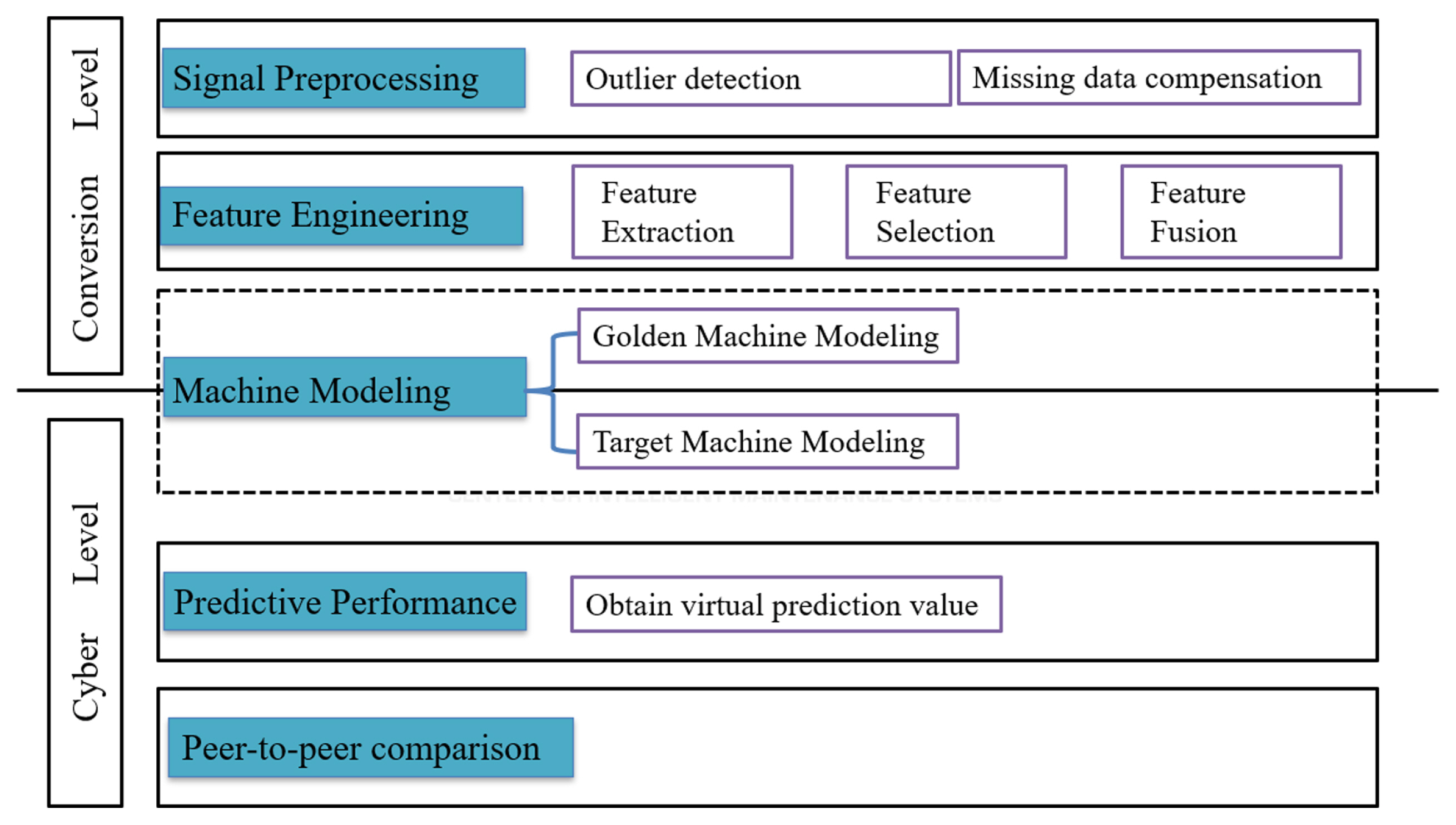
The material removal rate is an important criterion for judging the healthy state of the chemical-mechanical planarization process in semiconductor fabrication. This research has adopted the 2016 PHM society dataset [20]. This dataset mainly includes five types of variables: (1) Processing stage (2) Usage variable (i.e., Dresser usage, Polishing table usage); (3) Flow rate of slurry; (4) Rotation rate (i.e., wafer rotation rate); (5) Pressure of bag on the edge of the wafer. This dataset also includes ŌĆ£material removal rate (MRR)ŌĆØ as the label. According to the MRR distribution range, the dataset can be divided into low-speed and high-speed modes. This research has adopted a low-speed mode as the case study. We split the low-speed mode into two groups based on the processing stage. Table 1 shows the two groups used in this case. Group 1, low-speed mode stage B, is the golden machine. Group 2, low-speed mode stage A, is the target machine.
Fig. 3 represents the flowchart for this case studyŌĆÖs implementation to show the effectiveness of the proposed predictive methodology. The problem mentioned in this case study can be solved based on the proposed predictive metrology and traditional metrology methods. For predictive metrology, the first step is to acquire the signal data. After acquiring the signal, the time and frequency domain analysis are adopted.
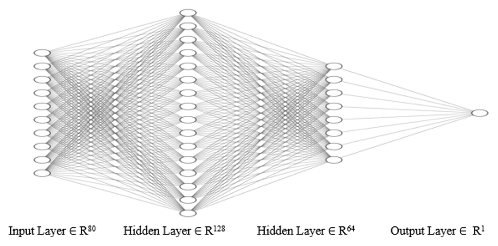
According to Section 3.1, the statistical features are extracted during this step, including the mean value, standard deviation, decreasing rate, area under the curve, time neighbor features, and usage neighbor features. According to Section 3.2, the relative feature selection and PCA methods are used for feature engineering. For machine modeling, model-based transfer learning is adopted based on the fully connected neural network shown in Figure 4. The data in 2-dimensional format is used as an input to the network. The dimension of the input is Nsp ├Ś Nft, where Nsp is the number of the samples (i.e., 815 and 300 in the group 1 and 2, respectively) and Nft is the selected features (i.e., 80 in the present case). Two hidden layers (i.e., the first and second layer has 128 and 64 neurons, respectively) have been used to map the features from the input to the output layer. The epochs used in the fully connected neural network is 60, and the learning rate is 10ŌłÆ5.
The traditional method takes the same step for data acquisition, data preprocessing, feature extraction and selection. The main difference between the proposed and traditional methods is whether to compare with the golden machine.
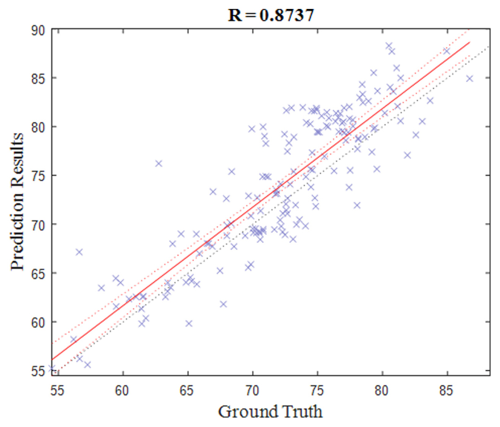
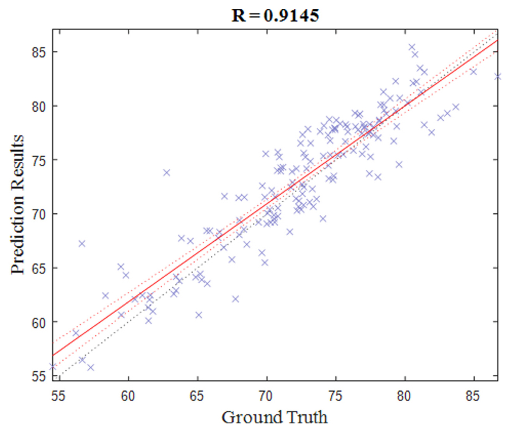
Table 2 shows the prediction results obtained based on both methods. Figs. 5 and 6 show the regression plots for both predictive metrology and traditional method, where Fig. 5 shows the prediction results obtained based on the predictive metrology method, and Figure 6 shows the prediction results obtained based on the direct modeling method. Comparing the proposed method with the traditional method, less mean square error in prediction has been observed based on the proposed method.
5. Conclusion
This paper presents a novel architecture that combines the predictive metrology concept and 5-level cyber-physical system (CPS) architecture. Predictive metrology can help solve the low-volume data issue in the target domain and better control the yield and quality in semiconductor manufacturing through peer-to-peer comparison. Based on testing results on the 2016 PHM public dataset, R-value in the proposed metrology model is 0.9145, and MSE is 7.52. R-value in the traditional method is 0.8737, and MSE is 16.23. The simulation results have proved that the proposed method is effective. The experiment will validate feasible machine calibration plans, health assessment, monitoring, and human-in-loop decision-making systems for future works.


 PDF Links
 PubReader
 Full text via DOI
 Download Citation
  CrossRef TDM


